
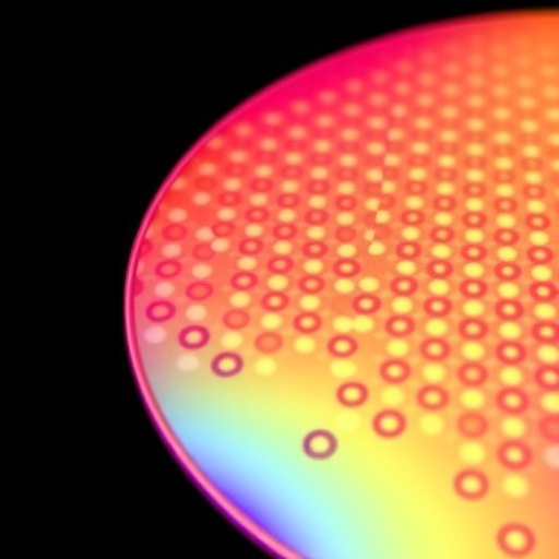
Making short-wave infrared cameras practical for everyday use may depend on solving a problem that is less visible than sensitivity but just as important: uniformity. A new study reports a directly synthesized p-type lead sulfide quantum-dot ink that can produce highly consistent infrared-sensitive films across six-inch silicon wafers. The advance could help transform SWIR imaging from a specialized technology into a scalable platform for traffic monitoring, autonomous vehicles, machine vision, environmental sensing and other applications where large arrays of pixels must perform reliably together.
Short-wave infrared, or SWIR, generally covers light wavelengths beyond the visible range and extending to approximately 2,500 nanometers. Although people cannot see this radiation, SWIR cameras can reveal information hidden from ordinary cameras, particularly in haze, fog and other conditions that reduce visible-light contrast. Lead sulfide, or PbS, quantum dots are among the most promising materials for affordable SWIR detectors because their optical properties can be tuned through particle size and surface chemistry. They can also be deposited from liquid inks using coating or printing methods compatible with large-area manufacturing.
The challenge is ensuring that every quantum-dot pixel responds in the same way. In a high-resolution imaging chip, thousands or millions of detectors operate side by side. If the light-sensitive layer varies in thickness, composition or electrical conductivity, some pixels may appear unusually bright, produce excessive noise or fail completely. Such pixel-to-pixel differences can undermine an entire imaging system, even when individual photodetectors demonstrate strong sensitivity in laboratory tests.
The research team focused on p-type PbS quantum dots, which are used together with n-type materials to form p–n junction photodetectors. These junctions separate the electrons and holes generated when the quantum dots absorb infrared photons, allowing the resulting electrical signal to be collected efficiently. While n-type quantum-dot inks have become comparatively mature, creating uniform p-type films over large areas has remained difficult.
Conventional p-type film fabrication usually involves solid-state ligand exchange. First, quantum dots are deposited to form a film. Their original surface molecules are then replaced with shorter or chemically different ligands that improve electrical transport and alter the material’s carrier type. However, the exchange reaction can proceed unevenly through the film. It may also cause the film to contract as bulky ligands are removed, creating cracks, thickness fluctuations and local variations in conductivity. These defects become increasingly serious as the coated area expands.
Instead of modifying the quantum dots after film deposition, the researchers developed a p-type PbS ink in which the desired surface chemistry is established during synthesis. By adjusting the functional groups of thiol-based ligands, they controlled how strongly the molecules interacted with the quantum-dot surfaces and how they influenced the material’s electronic behavior. The team also used a seeded-growth strategy, enabling the quantum-dot size and therefore the absorption wavelength to be adjusted over a broad range. The first excitonic absorption peak could be shifted from about 1,100 nanometers to beyond 2,000 nanometers, covering much of the SWIR region.
The direct-ink approach produced dense, crack-free films with strikingly improved thickness uniformity. Across six-inch silicon wafers, films made using conventional solid-state ligand exchange showed thickness variations of approximately plus or minus 7.82 nanometers. Films deposited from the directly synthesized p-type ink varied by only plus or minus 0.31 nanometers. The improvement was not limited to physical thickness. Surface-potential maps and sheet-resistance measurements showed that the electrical properties were also far more homogeneous, suggesting that the ink can provide a consistent foundation for wafer-level device fabrication.
The researchers then tested the material in SWIR photodetectors and prototype imaging modules. At the individual-device level, the new detectors performed comparably with conventional devices and showed lower noise in some measurements. The larger benefit emerged when many pixels were operated together. Photoresponse non-uniformity fell from 10.57 percent to 5.79 percent, while the proportion of dead pixels dropped from 0.21 percent to just 0.03 percent. In practical terms, this means that a greater fraction of the imaging array contributes useful data and that neighboring pixels are less likely to disagree simply because of variations in the film.
To illustrate the advantage under realistic conditions, the team paired its SWIR imager with an object-recognition algorithm designed to detect vehicles. In clear conditions, both visible and SWIR cameras supported reliable recognition. When fog reduced contrast in the visible images, however, the SWIR system preserved clearer information about the scene and achieved better recall and F1 scores. The findings suggest that directly synthesized p-type PbS inks could help deliver infrared cameras that are not only sensitive, but also uniform, manufacturable and robust enough for demanding real-world environments.
Subject of Research: Directly synthesized p-type lead sulfide quantum-dot inks for uniform wafer-scale short-wave infrared films and imaging devices
Article Title: Directly synthesized p-type quantum dot inks enable uniform wafer-scale SWIR films
Web References: https://doi.org/10.1093/nsr/nwag421
References: National Science Review, DOI: 10.1093/nsr/nwag421
Image Credits: © Science China Press
Keywords
Short-wave infrared, SWIR imaging, lead sulfide quantum dots, PbS quantum dots, p-type quantum-dot ink, photodetectors, wafer-scale films, infrared cameras, quantum-dot electronics, vehicle detection
Tags: high-resolution SWIR detector arraysinfrared imaging in fog and hazelarge-area quantum dot coatingsp-type lead sulfide quantum dotsquantum dot ink synthesisquantum dot ink uniformityquantum-dot-based SWIR sensorsscalable quantum dot material processingscalable SWIR imaging technologyshort-wave infrared camera developmentuniformity in quantum dot filmswafer-scale infrared sensor fabrication