
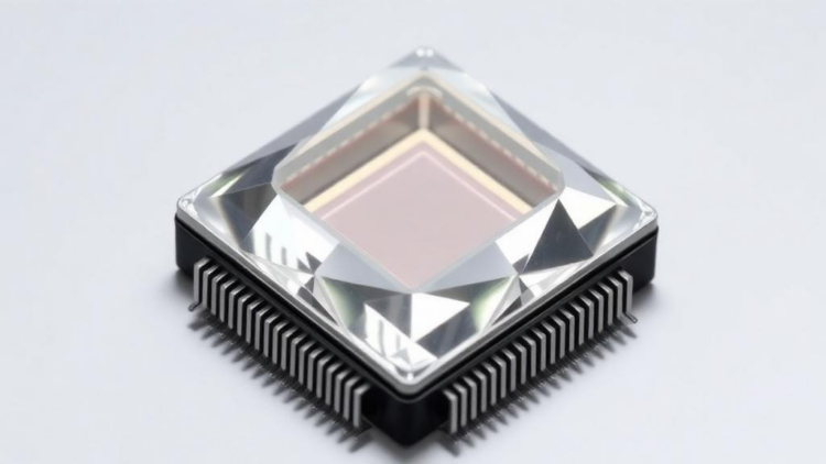
As the semiconductor industry pushes power densities to levels that would have seemed fantastical a decade ago, heat has quietly become the bottleneck that determines how fast, how dense, and how reliable our electronics can be. A comprehensive new review published in the Journal of Materials Science by researchers at the University of Electronic Science and Technology of China, working with the United Microelectronics Center, argues that the answer to this thermal crisis may lie in one of nature’s most remarkable materials: diamond. The review, led by Shihang Wu and Yuanfu Chen, weaves together diamond fundamentals, thermal transport theory, integration strategies across four major semiconductor platforms, and advanced packaging technologies into a single roadmap for the next generation of high-performance electronics.
The case for diamond begins with physics. Diamond possesses the highest thermal conductivity of any bulk material, reaching values far beyond copper or silicon, while simultaneously acting as an excellent electrical insulator. That combination is almost paradoxical: the material can pull enormous amounts of heat away from a transistor junction without conducting a single stray electron. Add outstanding thermo-mechanical stability and a coefficient of thermal expansion that can be managed through engineering, and diamond becomes uniquely suited to sit directly against the hottest, most power-hungry regions of a chip. In an era when three-dimensional integrated systems stack multiple dies on top of one another, trapping heat in layers where conventional cooling cannot reach, this near-junction heat extraction capability is precisely what the industry needs.
But the review is candid about the central obstacle: the thermal boundary resistance that arises wherever diamond meets another material. When heat flows across an interface between two solids, phonons—the quantum packets of vibrational energy that carry heat in insulators—scatter at the boundary due to differences in vibrational spectra, bonding, and crystal structure. This interfacial resistance can dominate the entire thermal budget of a device, sometimes negating the benefit of diamond’s extraordinary bulk conductivity. The authors trace the theoretical framework, rooted in the classic acoustic mismatch and diffuse mismatch models, and show how modern interface engineering—ultrathin interlayers, carbide-forming adhesion layers, and controlled amorphous transition regions—can dramatically reduce this resistance. Recent molecular dynamics studies, including work using machine-learned interatomic potentials, are now revealing how phonon bridge mechanisms and nanoscale structural transitions govern heat flow across these heterogeneous junctions.
The most mature application is the GaN-on-diamond platform. Gallium nitride high-electron-mobility transistors are the workhorses of radio-frequency and power electronics, but their performance is throttled by self-heating in a thin channel near the surface. Growing polycrystalline diamond directly onto GaN wafers, or bonding single-crystal diamond membranes to processed devices, moves the heat sink within micrometers of the hot spot. The review documents remarkable progress: room-temperature surface-activated bonding of GaN to diamond, carbide interlayers that achieve low thermal boundary resistance, and even all-around diamond integration of nanoscale gate-length devices. Record-low interfacial resistance has been reported at bonded GaN-diamond interfaces by controlling an ultrathin heterogeneous amorphous layer, and top-side diamond integration into AlGaN/GaN transistors demonstrates that diamond can now be placed on both sides of the active region.
Silicon, silicon carbide, and the emerging ultrawide-bandgap semiconductor beta-gallium oxide each present distinct integration challenges that the review addresses in turn. For silicon, the mismatch in thermal expansion and the chemical incompatibility of diamond growth conditions with silicon processing demand careful strategies, including ion-beam-activated hydrophilic bonding with aluminum nitride interlayers and atomic-level transition engineering to boost thermal boundary conductance. Silicon carbide, with its own high thermal conductivity, benefits from diamond-SiC engineered substrates that have already demonstrated enhanced heat dissipation in GaN transistors, though non-equilibrium molecular dynamics simulations continue to pinpoint the sources of residual interfacial resistance. Beta-gallium oxide, a material with enormous promise for power devices but notoriously poor thermal conductivity, may benefit most of all: researchers have grown polycrystalline diamond directly on it, demonstrated van der Waals thin-film integration, and even shown wafer-level transfer printing of beta-gallium oxide films and MOSFETs onto diamond substrates at the IEEE International Electron Devices Meeting.
Achieving these device-level wins requires a reliable supply of diamond itself, and the review devotes substantial attention to manufacturing. Chemical vapor deposition, particularly microwave plasma CVD, is the dominant route, and reactor design has become a science of its own, with multiphysics modeling and electromagnetic mode engineering now enabling four-inch deposition areas. Single-crystal diamond wafers, historically limited to a few millimeters, have grown to inch sizes through mosaic growth techniques that stitch together multiple seeds with precisely controlled crystallographic orientations, and heteroepitaxial growth on iridium buffer layers offers a scalable path to larger wafers. Perhaps most striking is the recent demonstration of scalable production of ultraflat, ultraflexible diamond membranes published in Nature, which opens the door to transferring thin diamond layers onto arbitrary substrates—the same logic that transformed silicon-on-insulator technology decades ago.
Beyond the chip, the review surveys a full arsenal of diamond-based packaging technologies. Diamond heat spreaders, long used in laser diodes and RF amplifiers, are now being combined with copper-diamond composites whose metal matrices are engineered with carbide coatings to maximize thermal conductivity. Diamond microchannel heat sinks represent the most aggressive approach: by etching or laser-machining channels directly into diamond and flowing coolant through them, researchers have demonstrated cooling of heat fluxes approaching the kilowatt-per-square-centimeter regime, with designs including zigzag double-layer channels, rhombus pin fins, and hybrid single-crystal-polycrystalline structures that direct heat away from hot spots. Two-phase flow boiling in diamond microchannels and in-chip microfluidic cooling on diamond substrates have both pushed wide-bandgap electronics to record-high heat fluxes, echoing the microfluidic cooling concepts first proposed for VLSI circuits in the 1980s but now realized in a far superior material.
For three-dimensional integration, the review highlights through-diamond vias and diamond interposers as the packaging equivalents of through-silicon vias, but with thermal performance that silicon cannot match. Bottom-up copper filling of high-aspect-ratio diamond through holes enables vertical electrical interconnection while the surrounding diamond conducts heat laterally and vertically. Diamond interposers have been demonstrated for 2.5D chiplet packaging in supercomputing applications, diamond-on-chip-on-glass architectures have shown efficient thermal management, and diamond-copper composite interposers are being explored for electric vehicle power modules. Warpage mitigation, a persistent headache in wafer-to-wafer bonding, is being tackled through heterogeneous integration of diamond heat spreaders, while hybrid copper-diamond microbump bonding points toward fully three-dimensional heterogeneous systems in which the thermal and electrical pathways are co-designed from the outset.
The review closes with a forward-looking agenda: wafer-scale diamond manufacturing that can feed standard semiconductor fabrication lines, advanced packaging flows that treat diamond as a first-class structural and thermal material rather than an afterthought, and system-level thermal design that co-optimizes materials, devices, and packaging from the transistor to the heat sink. The authors also note emerging applications beyond conventional electronics, including three-dimensional integration of diamond spin qubits for quantum computing and heterogeneous integration of spin-photon interfaces with CMOS platforms, where diamond’s role is not merely thermal but functional. If the integration challenges documented in this review can be overcome at scale, the industry may find that the oldest gemstone becomes the defining material of the hottest new technology of the century.
Subject of Research: Diamond heterogeneous integration and advanced packaging for thermal management of semiconductor devices
Article Title: Review: diamond heterogeneous integration for thermal management—integration strategies and advanced packaging
Article References: Wu, S., Wu, F., Zhang, J., Ji, J., Zhang, W., Luo, W., Shao, W., & Chen, Y. (2026). Review: diamond heterogeneous integration for thermal management—integration strategies and advanced packaging. Journal of Materials Science. https://doi.org/10.1007/s10853-026-13776-8
Image Credits: AI Generated
DOI: 10.1007/s10853-026-13776-8
Keywords: diamond, thermal management, heterogeneous integration, GaN, advanced packaging, thermal boundary resistance, microchannel heat sink, CVD diamond, power electronics, 3D integration, semiconductors, heat spreaders
Cite Scienmag News
APA MLA Chicago
Copy citation Download RIS
Tags: 3D integrationaddressing heat dissipation bottlenecks in electronicsadvanced packagingadvanced packaging technologies using diamondchallenges and strategies for implementing diamond in electronic devicesCVD diamonddiamondDiamond-based heat shields for high-performance semiconductor devicesGaNheat spreadersheterogeneous integrationhigh thermal conductivity materials for chip coolingintegration of diamond in semiconductor platformsmaterial innovation for semiconductor heat managementmicrochannel heat sinkovercoming thermal crisis in power-dense chipspower electronicsproperties of diamond as an electrical insulator and heat conductorroadmap for thermal solutions in electronics industrysemiconductorsthermal boundary resistancethermal managementthermal management in next-generation electronicsthermal transport theory in semiconductor materials