

Tokyo, Japan – The realm of electronics has long been dominated by transistors, devices that amplify and switch electrical signals, serving as the backbone of modern technology. Yet, as devices shrink and performance demands grow, the traditional silicon-based transistor approach reaches a critical crossroads. As research advances, the quest for materials that can enable further miniaturization and enhancement of performance has intensified. A research team at the Institute of Industrial Science, The University of Tokyo, has explored this fundamental challenge, leading to the development of a groundbreaking transistor that could fundamentally alter the landscape of electronic components.
In a pioneering study, the researchers have shifted their focus away from silicon, traditionally the stalwart material of transistor technology. Instead, they turned to gallium-doped indium oxide (InGaOx), a material that promises both superior performance and enhanced reliability. The unique characteristics of InGaOx, configured as a crystalline oxide, provide an optimal environment for electron mobility, paving the way for next-generation applications. This shift from silicon to gallium-doped indium oxide represents a significant evolution in material science, aiming to address the hurdles posed by conventional semiconductor materials.
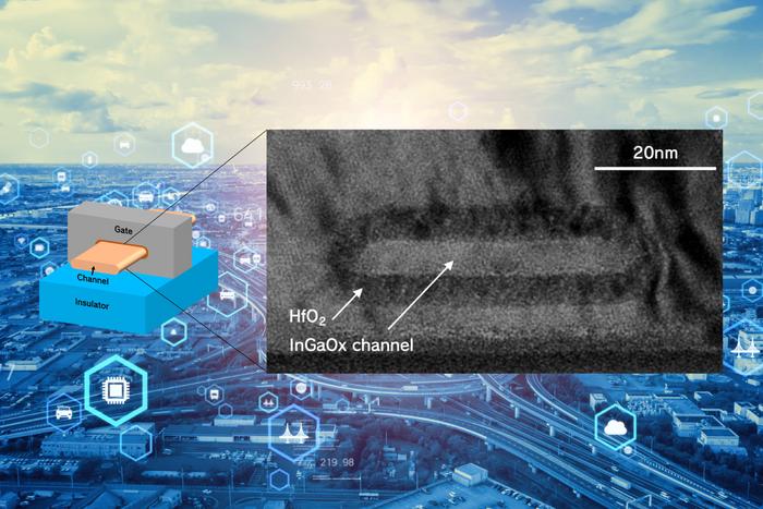
A critical aspect of their research was the structure of the transistor itself. The team introduced a gate-all-around configuration for the transistor, which ensures that the gate element, responsible for regulating the flow of current, envelops the channel through which electrons travel. This innovative arrangement enhances both efficiency and scalability, offering major advantages over traditional transistor architectures. The research team’s commitment to improving the electrical characteristics of their new device underpins their larger mission to redefine electronic component design and functionality.
.adsslot_ULAI4YushH{ width:728px !important; height:90px !important; }
@media (max-width:1199px) { .adsslot_ULAI4YushH{ width:468px !important; height:60px !important; } }
@media (max-width:767px) { .adsslot_ULAI4YushH{ width:320px !important; height:50px !important; } }
ADVERTISEMENT
The process of fabricating this advanced transistor involved a meticulous technique known as atomic-layer deposition. This method allowed the team to layer the gallium-doped indium oxide to the desired thickness, one atomic layer at a time. Not only does this enhance uniformity and control over the material properties, but it also facilitates the achievement of the necessary crystalline structure that optimizes electron drift and overall performance. The craftsmanship involved in this meticulous layering process is fundamental to the reliability and efficiency of the newly designed gate-all-around metal oxide-based field-effect transistor.
Dr. Anlan Chen, the lead author of the research, highlights the significance of achieving a high charge carrier mobility of 44.5 cm²/Vs with their transistor design. This metric, a critical indicator of performance in semiconductor devices, underscores the technological advancements made possible through their innovative use of InGaOx. The researchers’ findings demonstrate that their gate-all-around MOSFET significantly enhances device reliability and stability, operating effectively for nearly three hours under sustained stress. This reliability is a vital improvement when considering the demands of future electronic applications, especially in fields requiring enormous computational resources.
Moreover, the implications of this research extend beyond mere performance metrics. By addressing the inherent stability issues in indium oxide with gallium doping, the researchers have introduced a forward-looking approach to transistor design. In conventional silicon transistors, performance degradation due to operational stress can occur rapidly, leading to inefficiencies in electronic circuits. The team’s ability to minimize oxygen-vacancy defects in InGaOx coordinates a quest for reliable materials that maintain performance under pressure, positioning their transistor as a promising alternative to silicon in high-density electronic components.
The significance of such advancements becomes particularly salient when considering the rise of applications tied to artificial intelligence and big data analytics. In these sectors, the demand for reliable, high-performance electronic components continues to escalate, urging the scientific community to explore innovative materials and architectures. The tiny transistors designed by this research team are poised to meet these criteria, serving as integral components in the next generation of technology that can foster advancements in computational speed and efficiency.
Urbanization and the increasing sophistication of digital devices in everyday life compel material scientists and electrical engineers to critically pursue alternative semiconductor technologies. As traditional silicon-based technologies face limitations, the sophisticated gallium-doped transistors are an excellent representation of a paradigm shift in the field. The meticulous work by the Institute of Industrial Science researchers not only illustrates the technical feasibility of these materials but also inspires a generation of engineers to think critically about the materials they utilize in electronic devices.
This groundbreaking research will be showcased at the 2025 Symposium on VLSI Technology and Circuits, where experts from around the world will delve into the technical specifics and broader implications of such innovations. The dialogue at such forums often leads to collaborative efforts and further projects that can push the boundaries of existing technologies.
Looking into the future, as society progresses towards a more interconnected technological framework, the introduction of reliable and efficient electronic components becomes essential. The transistor technology developed by the University of Tokyo’s team has the potential to vastly upgrade the reliability and performance of consumer electronics, computer systems, and even smart devices that dominate our contemporary lifestyle. Such advancements are not merely incremental but represent a fundamental leap in how transistors interact with the technical landscape.
As the layers of research unravel the complexities of semiconductor performance, the implications of innovative structures and materials lead to a deeper understanding of the critical components that underpin modern electronics. The advanced transistors developed by the research team are not merely components; they embody the aspirations of a future where high-performing, reliable technology becomes the norm rather than the exception.
This research serves as a reminder that the journey of innovation is never-ending, and as one technology reaches its limits, another rises to take its place. As we prepare for an era dominated by advanced electronic systems and AI-driven technologies, studies like this one have profound significance for anyone invested in the future of electronic devices. The confluence of material science and engineering creativity marks a pivotal moment not just in electronics but also in the transformative potential of technology to reshape our lives.
This advancement not only enriches our current understanding of semiconductor technology but also solidifies the foundation for future breakthroughs. As researchers continue to explore the vast expanse of materials science, the promise of gallium-doped indium oxide MOSFETs leads us toward an exciting horizon where efficiency and reliability coexist, redefining the standards for electronic devices of the future.
Subject of Research: Development of Gallium-Doped Indium Oxide Transistors
Article Title: A Gate-All-Around Nanosheet Oxide Semiconductor Transistor by Selective Crystallization of InGaOx for Performance and Reliability Enhancement
News Publication Date: 6-Jun-2025
Web References:
References:
Image Credits: Credit: Institute of Industrial Science, The University of Tokyo
Keywords
Advanced Transistors, Gallium-Doped Indium Oxide, Electronic Components, Semiconductor Technology, Material Science, MOSFET, Electrical Engineering, Reliability, Performance Enhancement, VLSI Technology.
Tags: advanced transistors technologychallenges in silicon-based transistorscrystalline oxide transistorsfuture of transistor technologygallium-doped indium oxide applicationsInstitute of Industrial Science researchminiaturization of electronic componentsnext-generation semiconductor materialsperformance enhancement in transistorsreliability of advanced transistorsresearch in electronics materialstransistor gate-all-around configuration