
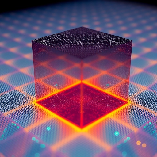
In a groundbreaking stride towards the future of optical computing, researchers have unveiled a transformative technology capable of revolutionizing how images are processed and manipulated entirely via light. This cutting-edge advance centers on what are called double-phase metasurface operators—ultrathin, engineered surfaces that can control light with exquisite precision. The scientific breakthrough promises profound implications for fields ranging from telecommunications to medical imaging and artificial intelligence, marking a new era where all-optical image processing can be both compact and highly efficient.
At the heart of this development lies the innovative design of metasurfaces, which are flat structures far thinner than conventional optical components yet able to modulate light’s phase, amplitude, and polarization at will. Traditionally, image processing tasks rely heavily on electronic computation, which introduces latency and energy inefficiencies. The newly devised double-phase metasurface operators bypass these limitations by harnessing the unique properties of light itself—effectively embedding mathematical operations within the metasurface’s nanoscale architecture. This approach allows for real-time, ultrafast image processing without converting optical signals back into electronic data.
The concept of a “double-phase” metasurface hinges on precise control over two phase profiles simultaneously. By engineering these carefully tailored phase patterns onto a single metasurface, the researchers can perform complex linear transformations on incident light fields, which equate to essential image processing functions such as spatial filtering, edge detection, and pattern recognition. This remarkable functionality is achieved within an exceptionally compact device footprint, making it highly suitable for integration in next-generation optical systems where size, weight, and power consumption are critical constraints.
One particularly compelling aspect of this new technology is the all-optical nature of the information processing. Conventional image processing methods typically involve converting photons into electrons, digitizing signals, and applying algorithms through electronic processors. In contrast, double-phase metasurface operators enable the entire process to remain in the optical domain, eliminating data conversion bottlenecks. This could dramatically accelerate processing speeds, reduce energy usage, and enable new modalities of dynamic, real-time image analysis that are currently unattainable through purely electronic means.
Applications of this technology are broad and impactful. In telecommunications, it could streamline the handling of optical signals, enhancing bandwidth efficiency and reducing latency in data centers or communication networks. In medicine, the ability to process images optically in ultra-compact formats could advance portable diagnostic devices or real-time tissue imaging during surgeries. Moreover, the versatility of these metasurfaces allows for dynamic reconfiguration, hinting at future smart optical components that adapt to different computational tasks on the fly without physical alterations.
The fabrication of these double-phase metasurface operators involves sophisticated nanomanufacturing techniques. Researchers pattern subwavelength dielectric structures on high-index materials, encoding intricate phase distributions with nanometric precision. The resulting metasurface manipulates the incoming light wavefront by introducing spatially varying phase shifts that correspond to the desired computational function. This precise engineering requires extensive computational modeling and optimization to ensure that the metasurface operates efficiently across the targeted wavelength range, minimizing losses and aberrations.
Critically, the research team demonstrated experimentally that these metasurfaces could realize essential image processing functions such as differentiation and integration, fundamental building blocks for edge detection and image smoothing, respectively. By cascading multiple metasurfaces or combining phase profiles, they could implement compound operations, opening avenues for highly sophisticated all-optical computing architectures. The experimental validation underscores the readiness of this technology for real-world applications, moving beyond theoretical proposals into prototyped functional devices.
Perhaps most exciting is the potential scalability and compatibility of double-phase metasurface operators with existing semiconductor manufacturing. Unlike bulky optical components or complex systems requiring precise alignment, these metasurfaces can be integrated onto chips or optical fibers, interfacing seamlessly with current photonic infrastructures. This synergy supports the vision of compact and robust optical processors embedded within everyday technology, from smartphones to machine vision systems, dramatically enhancing performance while slimming down hardware footprints.
The implications for artificial intelligence are also profound. Many AI applications rely on rapid image recognition and pattern analysis, traditionally constrained by electronic processing speeds and power consumption. Employing metasurface-based optical computation could empower AI systems with instantaneous, energy-efficient image preprocessing, accelerating neural network inference and enabling novel real-time sensory processing. This convergence of photonics and AI heralds a paradigm shift, where optical devices themselves contribute to intelligent information processing.
Another intriguing facet of the research lies in the tunability and reconfigurability potential of metasurfaces. Although the current implementation relies on static phase patterns, future iterations may incorporate materials responsive to external stimuli—such as electrical signals, temperature shifts, or light intensity—enabling dynamically programmable optical operators. Such devices would usher in versatile, adaptive processing platforms capable of switching functionalities without physical replacement, substantially broadening the utility and impact of metasurface-based optical computing.
Despite these promising advancements, several challenges remain before widespread adoption. Ensuring fabrication consistency at scale, managing losses introduced by nanoscale structures, and achieving broad spectral bandwidth remain active areas of investigation. Furthermore, integrating these metasurfaces into larger optical systems requires overcoming alignment tolerances and interfacing with other photonic components. Nonetheless, the rapid progress illustrated by this research roadmap suggests these hurdles will be addressed in near future, propelling metasurface optics into mainstream technological applications.
In summary, the emergence of double-phase metasurface operators marks a significant leap forward in the field of optical information processing. By embedding complex computational functionalities directly into ultra-thin nanoscale structures, these metasurfaces facilitate ultrafast, energy-efficient all-optical image processing, circumventing traditional electronic bottlenecks. As fabrication techniques mature and integration challenges are overcome, this technology is poised to unlock new horizons across communication, medical imaging, artificial intelligence, and beyond, transforming how we manipulate and harness light for computing tasks.
As the scientific community continues to push the boundaries of metasurface capabilities, this landmark research embodies the convergence of nanotechnology, photonics, and information science. It exemplifies how innovative material engineering and design can revolutionize established paradigms, inspiring future explorations into the untapped potential of light-based computing. Within a decade, the seamless marriage between metasurface optics and all-optical computing may well catalyze a technological renaissance, delivering unprecedented processing speed, miniaturization, and adaptability.
Reflecting on this profound innovation, one is reminded that the future of image processing may no longer rest purely in silicon and electrons, but increasingly in the ethereal manipulation of photons through engineered surfaces. The work of Yu, Singh, Pietila, and colleagues signals the dawn of this exciting transition, heralding a future where light itself becomes the medium, the messenger, and the processor of information at the speed of nature’s fastest messenger.
Article References:
Yu, L., Singh, H.J., Pietila, J. et al. Double-phase metasurface operators for all-optical image processing. Light Sci Appl 15, 119 (2026). https://doi.org/10.1038/s41377-025-02153-w
Tags: all-optical image processingartificial intelligence optical systemsdouble-phase metasurfacesenergy-efficient image processinglight phase modulationmedical imaging innovationmetasurface mathematical operationsnanoscale light controloptical computing advancementsoptical telecommunications technologyreal-time image manipulationultrathin optical components