
Scientists Achieve Unprecedented Visualization of Nanoscale Charges at Ferroelectric Domain Interfaces
In a groundbreaking advancement that promises to revolutionize our understanding of ferroelectric materials, a team of researchers at the University of Tokyo has successfully captured the elusive charge distributions at the nanoscale ferroelectric domain interfaces. This pioneering research addresses a long-standing challenge in materials science by employing cutting-edge electron microscopy techniques capable of observing both atomic displacements and localized charges at an ultra-fine scale. The findings, published on June 13, 2025, in the prestigious journal Science Advances, provide unprecedented insights into the fundamental behavior of ferroelectric domain walls and are poised to impact the development of next-generation electronic components.
Ferroelectric materials are distinguished by their spontaneous electrical polarization, which can be reversed under the application of an external electric field. These materials are composed of numerous domains—regions where the polarization is uniformly oriented—and are separated by domain interfaces. The electrical properties of these interfaces, which are minuscule yet crucial boundaries, dictate how domain walls move and interact, ultimately influencing the performance of devices such as multilayer ceramic capacitors (MLCCs). Despite their significance, direct experimental observation of the charges trapped at these domain boundaries has remained a formidable challenge, primarily due to the atomic scale and complexity of interactions involved.
.adsslot_YtBLkF9sEe{ width:728px !important; height:90px !important; }
@media (max-width:1199px) { .adsslot_YtBLkF9sEe{ width:468px !important; height:60px !important; } }
@media (max-width:767px) { .adsslot_YtBLkF9sEe{ width:320px !important; height:50px !important; } }
ADVERTISEMENT
Multilayer ceramic capacitors, ubiquitous in modern electronic devices including smartphones, personal computers, and automotive systems, rely heavily on ferroelectric ceramics for their high capacitance and reliability. As consumer electronics evolve towards smaller sizes with enhanced capabilities, understanding and controlling ferroelectric domain behavior becomes imperative. These MLCCs consist of alternating layers of ferroelectric materials and electrodes, housing myriad domains and domain walls at the nanometer scale. Variations in polarization across these domain interfaces lead to the accumulation of bound charges, which can have profound effects on leakage currents and device longevity. Thus, unraveling the charge states at domain interfaces is essential for optimizing device design and function.
The research led by Dr. Takehito Seki leveraged a combination of advanced electron microscopy methodologies, integrating localized charge observations with atomic-scale structural measurements. This technique enables visualization not only of the atomic positions with picometer precision but also of the polarization-induced charges confined within nanometric domain walls. The study’s achievement effectively bridges the gap between structural characterization and electrical property analysis, a correlation that until now was mostly theoretical or indirect in nature. Such direct observations usher in a new era for materials science, where the intricate coupling between atomic displacements and electronic polarization can be empirically examined.
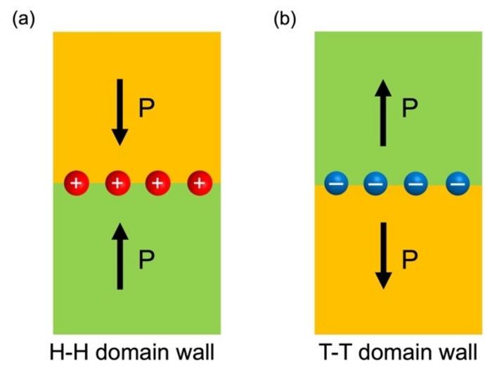
Importantly, the experiment identified and differentiated between head-to-head (H-H) and tail-to-tail (T-T) domain walls at the nanoscale. These domain configurations host oppositely charged polarization bound charges at their cores—positive charges in the former and negative in the latter. These localized charges necessitate electrical compensation from neighboring charges to maintain overall neutrality, influencing domain wall stability and mobility. Given that domain wall dynamics under applied voltages govern the ferroelectric switching properties that make these materials technologically attractive, the ability to observe charge distribution directly allows researchers to conceptualize mechanisms that govern device reliability and efficiency.
At the heart of this research lies the development of an “ultra” atomic resolution electron microscopy technique, a concept realized within the ERATO SHIBATA project, funded by the Japan Science and Technology Agency (JST). This novel microscopy transcends conventional resolution limits by combining structural and electromagnetic field imaging, even under variable temperature conditions ranging from extremely low to high temperatures. The capacity to observe the simultaneous evolution of atomic arrangements and electromagnetic phenomena offers unprecedented insights into material and biological functions that were previously inaccessible.
Furthermore, the elucidation of polarization-induced charge at ferroelectric domain interfaces aids in understanding leakage current generation, a persistent challenge affecting the reliability of ferroelectric devices. Leakage currents arise due to the movement or reconfiguration of domains and the associated free charge carriers. By mapping charge distributions with atomic precision, this study lays the groundwork for engineering domain walls with tailored properties that minimize parasitic currents and enhance device stability and lifespan. This has direct implications for the performance of MLCCs and other ferroelectric-based applications, from sensors to non-volatile memories.
Dr. Seki’s team employed specialized electron microscopy to observe atomic displacements in the sub-picometer range while simultaneously detecting charge accumulation at domain walls. This methodological feat was enabled by integrating physical models with high-resolution imaging, overcoming previous limitations that confined analyses to either structural or electrical domains. The researchers’ success opens pathways for exploring dynamic phenomena, such as domain wall motion and polarization switching, in situ under various external stimuli—a major leap toward functional characterization of ferroelectric materials.
This advancement is instrumental for the continued miniaturization and enhancement of electronic devices, as it uncovers the physical foundations underlying the domain wall behaviors that dictate device performance. The ability to “see” charge accumulation and atomic shifts together allows prototypes and materials to be optimized at an unprecedented level of detail, potentially informing the design of ferroelectric devices that are not only more compact but also more efficient and reliable.
Looking forward, this research heralds the possibility of direct “visualization” of fundamental physical processes that govern the function of a vast array of materials. By revealing the interplay between atomic-scale polarization patterns and local charge compensation mechanisms, it invites new theories and computational models to accurately predict the behavior of ferroelectric devices under operational conditions. This enhanced understanding promises to accelerate breakthroughs in a wide range of applications, including energy harvesting, capacitors, memory devices, and advanced sensors.
The significance of this breakthrough extends beyond ferroelectrics alone. The measurement principles and microscopy techniques developed may be adapted to other complex oxides and functional materials where nanoscale charge distributions govern macroscopic functionality. This could transform fields such as catalysis, superconductivity, and even biomaterials research, where electromagnetic interactions at the atomic level critically influence material performance.
In summary, the successful real-space observation of polarization-induced charges at nanoscale ferroelectric interfaces represents a landmark achievement in condensed matter physics and materials engineering. By marrying unprecedented imaging resolution with electrical characterization, the researchers have provided invaluable insights into domain wall physics and ferroelectric device operation. The implications for the future development of compact, high-performance, and highly reliable electronic components are profound and far-reaching.
This research was conducted under the auspices of the JST Strategic Basic Research Program ERATO project “SHIBATA Ultra-atomic Resolution Electron Microscopy,” reflecting a concerted national effort to push the boundaries of measurement science. By developing techniques that can simultaneously observe atomic structures and electromagnetic fields across wide temperature ranges, the project exemplifies how innovative tools can transform fundamental science and pave the way for technological leaps.
As electronic devices continue to shrink and demand ever greater capabilities, the insights provided by this study will be instrumental in driving innovation. The newly acquired ability to directly measure and interpret local charges at ferroelectric domain walls will not only enhance our fundamental understanding of ferroelectricity but will serve as a crucial foundation for engineering the next generation of energy-efficient, durable, and multifunctional electronic components.
Subject of Research:
Not applicable
Article Title:
Real-space observation of polarization induced charges at nanoscale ferroelectric interfaces
News Publication Date:
13-Jun-2025
Web References:
http://dx.doi.org/10.1126/sciadv.adu8021
Image Credits:
Naoya Shibata
Keywords
Ferroelectric materials, domain walls, polarization charges, multilayer ceramic capacitors, electron microscopy, nanoscale imaging, atomic displacement, leakage current, materials science, advanced characterization, SHIBATA project, Japan Science and Technology Agency
Tags: charge distribution visualization techniquesdomain walls and electrical propertieselectron microscopy in materials scienceexperimental observation of charge trappingferroelectric materials researchfundamental behavior of ferroelectric domain wallsmaterials science challenges in ferroelectricsmultilayer ceramic capacitors performancenanoscale ferroelectric domain interfacesnext-generation electronic components developmentspontaneous electrical polarization in materialsUniversity of Tokyo research advancements